Thursday, September 8, 2016

UVM Interview Questions Part 1

1.Explain function new and super.build in UVM.
2.Connect virtual interface in driver build_phase.
3.Explain config_db and resource_db.
4.Explain report phase in UVM.
5.Explain raise objection.
6.Explain global stop request.
7.Difference between object and component.
8.Difference between TLM 1.0 and TLM 2.0
9. Difference between Create() and New() ?
10. Can we have user defined phase in UVM?
11. What is analysis port?
12. What is TLM FIFO?
13. How sequence starts?
14. What is the advantage of  'uvm_component_utils() and `uvm_object_utils() ?
15. What is objection?
16. What are the benefits of using UVM?
17. What is the difference between Active mode and Passive mode?
18. What is the difference between copy and clone?
19. What is factory?
20. What are the types of sequencer? Explain each?
21. What are the different phases of uvm_component? Explain each?
22. How set_config_* works?
23. What is super keyword? What is the need of calling super.build() and super.connect()?
24. What is the different between set_config_* and uvm_config_db ?
25. What  are the different  override types?
26. What is virtual sequence and virtual sequencer?
27. Explain end of simulation in UVM?
28. How to declare multiple imports?
29. What is symbolic representation of port, export and analysis port?
30. What is the difference in usage of $finish and global stop request in UVM?
31. What is the difference between `uvm_do and `uvm_ran_send?
32. Why we need to register class with uvm factory?
33. diff between uvm_transaction and uvm_seq_item?
34. can we use set_config and get_config in sequence ?
35. What is uvm_heartbeat ?


some more set questions will be posted very soon.
         

System Verilog Interview Questions Part 1

1.Difference between int and integer.
2.Difference between bit [7:0] and byte.
3.Significance of logic data type?
4.Advantage of using dynamic array?
5.Difference between dynamic array, queue and associative array?
6.Difference between verilog and systemverilog.
7.What is static and dynamic objects in testbench?
8.Why can’t we use interface instead mailbox?
9.What is callback?
10.What is casting? How it works?
11.Explain polymorphism with an example.
12.What is encapsulation?
13.Question regarding stratified event queue how blocking and non-blocking assignments happens in verilog.
14.What is the use of modports?
15.What is input clock skew and output clock skew?
16.Difference between function and task.
17.How to randomize a variable though it is not declared as rand/randc?
18.How this array works arry [*] [$] [ ].
19.features of SV.
20.What is the limitation of randc?
21.Declaring a variable as rand, how to make use of that variable to work as randc.
22.Explain about ignore bins.
23.Explain code coverage.
24. Difference between task and  function?
25. Difference between Final and Initial block?
26. What is Bin?
27. What are void function?
28. What is difference between program and module?
29. What is difference between code coverage and functional coverage?


Digital Design Interview Questions Part 1

1.What is Synthesis?
2.Simplify the equation x' + xy.
3.Design xor gate using muxes.
4.Difference between Mealy and Moore fsm.
5.Design an fsm for sequence detector 1001.
6. A ring counter having 10 pulses .how many flip-flops  needed ?
7. How many minimum number of gates required to implement Half adder ?
   tp =10ns,ts=6ns,th=2ns, calculate clock frequency.

We have covered some more questions in below post.
http://basicsofvlsi.blogspot.in/2011/01/digital-design-interview-questions.html?m=1

Wednesday, September 7, 2016

Analog Interview Questions Part 1

1. Why do we prefer to use MOSFET over BJTs for VLSI circuits?
2. What are the various regions of operation of MOSFET? How are those regions used?
3. What is threshold voltage?
4. Explain the three regions of operation of a MOSFET.
5. What is channel-length modulation?
6. Explain depletion region?
7. What is body effect?
8. Give various factors on which threshold voltage depends.
9. Give the Cross-sectional diagram of the CMOS.
10. What is the fundamental difference between a MOSFET and BJT ?
11. Why are most interrupts active low?
12. Which is better: synchronous reset or asynchronous reset signal?
13. Why is the number of gate inputs to CMOS gates (e.g. NAND or NOR gates)usually limited to four?
14.What are the important aspects of VLSI optimization?
Power, Area, and Speed.
15.What are the sources of power dissipation?
16.What is the need for power reduction?
17.Give some low power design techniques.
18.Give a disadvantage of voltage scaling technique for power reduction.
19.Give an expression for switching power dissipation.
20.Will glitches in a logic circuit cause power wastage?
21.What is the major source of power wastage in SRAM?
22.What is the major problem associated with caches w.r.t low power design? Give techniques to overcome it.


Tuesday, October 18, 2011

FPGA Interview Questions


1. What is the full form of RTL?
2. What is the difference between RTL and HDL?
3. Draw the state diagram to detect a sequence?
4. Draw the state diagram of a traffic light controller?
5. Which one is faster Carry look ahead or ripple carry adder?
6. What is the difference between Big Endean format and Little Endean format?
7. Can you model SRAM at RTL level?
8. What do you mean by concurrent statement?
9. Define component instantiation?
10. What is the difference between variable and signal?
11. List some sequential statements?
12. Define a test bench?
13. What are the advantages of test benches?
14. What is the difference between behavioral simulation and timing simulation?
15. Does frequency of operation depend on critical path in a circuit? Justify?
16. What is slack?
17. What are different types of scaling? Which one is used and why?
18. What are the different design styles in VLSI?
19. What is the full form of ABEL?
20. What is entry delay and exit delay?
21. What is Controllability and Observability in testing?
22. What is fault coverage?
23. What is DFT? What is its importance?
24. Expand BIST? Explain?
25. What is the difference between testing and verification?
26. Given a circuit with a fault you have to find the test vector to detect that fault?
27. Consider a counter. I want it to sense odd pulses or even pulses (alternate pulses).How will you do it?
28. What is Synthesis?
29. What are set up time & hold time constraints? What do they signify? Which one is critical for estimating maximum clock frequency of a circuit?
30. What’s the critical path in a SRAM?
31. Draw the timing diagram for a SRAM Read. What happens if we delay the enabling of Clock signal?
32. Draw a 6-T SRAM Cell and explain the Read and Write operations
33. Draw the SRAM Write Circuitry
34. Approximately, what were the sizes of your transistors in the SRAM cell? How did you arrive at those sizes?
35. How will you allocate your time between architecture, coding, and verification?
36. How do you differentiate between coding in C/C++ and at RTL (Register Transfer Level) ?
37. How to implement Half-adder and full-adder in RTL?
38. When the latches are inferred in RTL ?


VLSI FPGA Design & Verification Questions


1. What is FPGA ?
2. What is the significance of FPGAs in modern day electronics?
3. What is Synthesis?
4. FPGA design flow?
5. Tell me some features of FPGA you are currently using?
6. What is LUT?
7. What value is inferred when multiple procedural assignments made to the same reg variable in an always block?
8. Can you explain what ‘stuck at zero’ means?
9. How to generate clocks on FPGA?
10. What are DCM’s? Why they are used?
11. How do you implement DCM?
12. Why is map-timing option used?
13. What are different types of timing verifications?
14. What is FPGA you are currently using and some of main reasons for choosing it?
15. Given two ASICs. one has setup violation and the other has hold violation. how can they be made to work together without modifying the design?
16. What is LVs and why do we do that. What is the difference between LVS and DRC?
17. What is minimum and maximum frequency of DCM in spartan-3 series fpga?
18. What is the purpose of a constraint file what is its extension?
19. Tell me some of timing constraints you have used?
20. Can you list out some of synthesizable and non synthesizable constructs?
21. When are DFT and Formal verification used?
22. Can you draw general structure of fpga?
23. What are different types of FPGA programming modes?what are you currently using ?how to change from one to another?
24. How many global buffers are there in your current fpga what is their significance?
25. What is gate count of your project?
26. Can you suggest some ways to increase clock frequency?
27. What is the significance of contamination delay in sequential circuit timing?
28. Suppose for a piece of code equivalent gate count is 600 and for another code equivalent gate count is 50,000 will the size of bitmap change? In other words will size of bitmap change it gate count change?
29. What do conditional assignments get inferred into?
30. What are different types of FPGA programming modes? What are you currently using ? How to change from one to another?
31. What logic is inferred when there are multiple assign statements targeting the same wire?
32. Compare PLL & DLL ?
33. How to achieve 180 degree exact phase shift?
34. We need to sample an input or output something at different rates, but I need to vary the rate? What’s a clean way to do this?
35. What is slice? What is CLB?
36. Can a CLB configured as ram?
37. What is the purpose of DRC?
38. What is frequency of operation and equivalent gate count of u r project?
39. What are the differences between FPGA and CPLD?
40. Draw a rough diagram of how clock is routed through out FPGA?
41. What is DFT ?
42. What is FPGA you are currently using and some of main reasons for choosing it?
43. Draw a rough diagram of how clock is routed through out FPGA?
44. What is SOPC Builder?
45. How do you implement the GCLK when there is lack of Source?
46. What are the latest FPGAs you like?Why?
47. What is a SoC (System On Chip), ASIC, “full custom chip”, and an FPGA?
48. How do you measure the size and density of various programmable logic devices?
49. What is soft processor? What is hard processor?
50. What is meant by 90nm technology?
51. What are the different forms of pull up?
52. What do you mean by translation and mapping?
53. What do you mean by speed grade?
54. What is the difference between ASIC Design and FPGA Design?
55. Setup time and hold time in digital circuits.
56. False path in FPGA’s, Critical path, Negative slack, Jitter vs. clock skew .
57. Routing delay, Flop to out delay, Flop to flop delay, Pad to flop delay, Board delay.
58. Knowledge of Synthesis and layout constraints.


Saturday, January 15, 2011

Digital design Interview Questions

  • If inverted output of D flip-flop is connected to its input how the flip-flop behaves?
  • Design a circuit to divide input frequency by 2?
  • Design a divide by two counter using D-Latch.
  • Design a divide-by-3 sequential circuit with 50% duty cycle.
  • What are the different types of adder implementation?
  • Draw a Transmission Gate-based D-Latch?
  • Give the truth table for a Half Adder. Give a gate level implementation of the same.
  • Design an OR gate from 2:1 MUX.
  • What is the difference between a LATCH and a FLIP-FLOP?
  • Design a D Flip-Flop from two latches.
  • Design a 2 bit counter using D Flip-Flop.
  • What are the two types of delays in any digital system
  • Design a Transparent Latch using a 2:1 Mux.
  • Design a 4:1 Mux using 2:1 Mux's.
  • What is metastable state? How does it occur?
  • What is metastablity?
  • Design a 3:8 decoder
  • Design a FSM to detect sequence "101" in input sequence
  • Convert NAND gate into Inverter in two different ways.
  • Design a D and T flip flop using 2:1 mux only.
  • Design D Latch from SR flip-flop.
  • Define Clock Skew, Negative Clock Skew, Positive Clock Skew?
  • What is race condition? How it occurs? How to avoid it?
  • Design a 4 bit Gray Counter?
  • Design 4-bit synchronous counter, asynchronous counter?
  • Design a 16 byte asynchronous FIFO?
  • What is the difference between a EEPROM and FLASH?
  • What is the difference between a NAND-based Flash and NOR-based Flash?
  • Which one is good: asynchronous reset or synchronous reset? Why?
  • Design a simple circuit based on combinational logic to double the output frequency.
  • What is the difference between flip-flop and latch?
  • Implement comparator using combinational logic, that compares two 2-bit numbers A and B. The comparator should have 3 outputs: A > B, A < a =" B.">
  • Give two ways of converting a two input NAND gate to an inverter?
  • What is the difference between mealy and moore state-machines?
  • What is the difference between latch based design and flip-flop based design?
  • What is metastability and how to prevent it?
  • Design a four-input NAND gate using only two-input NAND gates.
  • Why are most interrupts active low?
  • How do you detect if two 8-bit signals are same?
  • 7 bit ring counter's initial state is 0100010. After how many clock cycles will it return to the initial state?
  • Design all the basic gates NOT, AND, OR, NAND, NOR, XOR, XNOR using 2:1 Multiplexer.
  • How will you implement a full subtractor from a full adder?
  • In a 3-bit Johnson's counter what are the unused states?
  • What is difference between RAM and FIFO?
  • What is an LFSR? List a few of its industry applications.
  • Implement the following circuits:
    (a) 3 input NAND gate using minimum number of 2 input NAND gates
    (b) 3 input NOR gate using minimum number of 2 input NOR gates
    (c) 3 input XNOR gate using minimum number of 2 input XNOR gates assuming 3 inputs A,B,C?
  • Design a D-latch using (a) using 2:1 Mux (b) from S-R Latch?
  • How to implement a Master Slave flip flop using a 2 to 1 mux?
  • How many 2 input xor's are needed to inplement 16 input parity generator?
  • Convert xor gate to buffer and inverter.
  • Difference between onehot and binary encoding?
  • What are different ways to synchronize between two clock domains?
  • How to calculate maximum operating frequency?
  • How to find out longest path?
  • How to achieve 180 degree exact phase shift?
  • What is significance of ras and cas in SDRAM?
  • Tell some of applications of buffer?
  • Implement an AND gate using mux?
  • What will happen if contents of register are shifter left, right?
  • What is the basic difference between analog and digital design?
  • What advantages do synchronous counters have over asynchronous counters?
  • What types of flip-flops can be used to implement the memory elements of a counter?
  • What are the advantages of using a microprocessor to implement a counter rather than the conventional method (flip-flop and logic gates)?
  • What is the principal advantage of Gray Code over straight (conventional) binary?
  • What does Pipelining do?
  • Design divide by 2, divide by 3 circuit with equal duty cycle.
  • How many 4:1 mux do you need to design a 8:1 mux?
  • What is D-Word, Q-word?
  • Define Moore, Mealy state machines. Which one is good for timing?
  • Design a FSM to detect 10110. What is the minimum number of flops required?
  • Design a simple circuit based on combinational logic to double the output frequency.
  • Design a 2bit up/down counter with clear using gates. (No verilog or vhdl)
  • Design a finite state machine to give a modulo 3 counter when x=0 and modulo 4 counter when x=1.
  • Minimize: S= A' + AB
  • What is the function of a D-flipflop, whose inverted outputs are connected to its input?
  • How to synchronize control signals and data between two different clock domains?
  • Describe a finite state machine that will detect three consecutive coin tosses (of one coin) that results in heads.
  • In what cases do you need to double clock a signal before presenting it to a synchronous state machine?
  • How many bit combinations are there in a byte?
  • What are the different Adder circuits you studied?
  • Give the truth table for a Half Adder. Give a gate level implementation of the same.
  • Convert 65(Hex) to Binary
  • Convert a number to its two's compliment and back.
  • What is the 1's and 2's complement of the decimal number 25.
  • If A?B=C and C?A=B then what is the boolean operator ?

Thursday, July 22, 2010

Digital System and Binary Numbers

Digital Systems:
I have got many emails from students regarding  Digital System and Binary Numbers conecpts so this is quick review what is Digital System and Binary Numbers? and what it does.....i think it will help u guys...if u guys really intersted and want to become logical designer Download this book Digital Design (4th Edition) only book that can tech u basics in professional way recommended by many designers...
 Digital systems are used in:
  1. Communication
  2. Business transaction
  3. Traffic Control
  4. Medical treatment
  5. Internet
The signals in digital systems use just two discrete values: a binary digit. Binary digit
called a bit, has two values: 0 or 1.
Example: The decimal digits a through 9 are represented in digital system with a code
of four bits (e.g. is represented by 0111, 8 is represented by 1000, 9 is represented by
1001).

Binary Numbers
  • Decimal number:
         The decimal number system is said to be of base, or radix, '10' because it uses 10 digits
          (0, 1, 2, 3, 4, 5, 6, 7, 8, 9).

Example:
The decimal number 245 may be written as
2x10²+4x101+5x100
where 2, 4, and 5 are the coefficients. 
  • Binary Number System: 
         The coefficients of the binary number have only two possible values: '0' or '1'.

Example:
(1001)2 its equivalent decimal number is : 1x23+0x22+0x21+1x20 = 8 + 0 + 0 + 1 = 9
where 1, 0, 0, and 1 are the coefficients. 
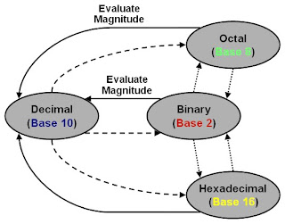
  • Octal number system (Base 8):
         The octal number system is said to be of base, or radix, '8' because it uses digits
   (00, 01, 02, 03, 04, 05, 06, 07, 10, 11, 12, 13, 14, 15, 16, 17). 
  • Hexadecimal number system (Base 16):
          It uses 16 digits : (0, 1, 2, 3, 4, 5, 6, 7, 8, 9, A, B, C, D, E, F). The letter A, B, C, D, E,
  and F are used for the digits 10,11, 12, 13, 14, and 15 respectively.

Example:
(124)16 = 1x162 + 2x161 + 4x160= 256 + 32 + 4 = 292


NUMBER BASE CONVERSION


Decimal to Binary conversion
  1. Divide the number with base '2'.
  2. Take the remainder 0 or 1 as a coefficient.
  3. Take the quotient and repeat the division.


Decimal to Octal conversion


Binary to Octal conversion

 Binary to Hexadecimal


Octal to Hexadecimal conversion


Complements:


The meaning of complement is something required to make a thing complete. For example, salsa complements tortilla chips, beer complements pizza, an ice cream cone complements a hot summer day, and apple sauce complements pork chops. A key concept to explore is how two things complement each other. For example, when a piece of pizza is removed from a whole pizza the piece complements what is left behind and vice versa. Each of the 4 following complements use the same concept except in different bases and what is considered a complete number in that base.

  • 1’s Complement: 
         The 1’s complement finds whatever is needed to make an entire set of 1’s. This is shown in the


  •  2’s ComplementFinding the 8 digit 2’s complement of 01101100
  • 9’s ComplementThe 9’s complement finds whatever is needed to make an entire set of 9’s. This is shown in the    
  • 10’s ComplementFinding the 5 digit 10’s complement of 1357 
      

Basic Logic Gate

         A logic gate performs a logical operation on one or more logic inputs and produces a single logic output. The logic normally performed is Boolean logic and is most commonly found in digital circuits. Logic gates are primarily implemented electronically using diodes or transistors, but can also be constructed using electromagnetic relays (relay logic), fluidic logic, pneumatic logic, optics, molecules, or even mechanical elements.

       In electronic logic, a logic level is represented by a voltage or current, (which depends on the type of electronic logic in use). Each logic gate requires power so that it can source and sink currents to achieve the correct output voltage. In a pure logic diagram logic levels and power supply connections do not exist and are not shown, but in a full logic circuit diagram, documenting the implementation of the logic, these are required.


      All other types of Boolean logic gates (i.e., AND, OR, NOT, XOR, XNOR) can be created from a suitable network of NAND gates. Similarly all gates can be created from a network of NOR gates. Historically, NAND gates were easier to construct from MOS technology and thus NAND gates served as the first pillar of Boolean logic in electronic computation.


     Truth table is a table that describes the behaviour of a logic gate or any combination of logic gates. It lists the value of the output for every possible combination of the inputs and can be used to simplify the number of logic gates and level of nesting in an electronic circuit. In general the truth table does not lead to an efficient implementation; a minimization procedure, using Karnaugh maps, the Quine–McCluskey algorithm or an heuristic algorithm is required for reducing the circuit complexity.

Truth table & Symbols


Friday, July 2, 2010

32x8 FIFO

FIFO is nothing but simple queue like we standing in cinema theaters.one who standing first will get ticket last guy may or may not...this is concept.in technical 32x8 fifo is 32 locations with each location can accommodate 8 bit data...in this writeptr and readptr plays very important role...operation starts when write enables data stores into reg and startes incriment writeptr..after completion write operation we have to enable read operation..when read is enabled readptr starts incrimenting and extract data from register....

module fifo2 (dout,enb1, wrtenb, redenb, clk, rst, out,wrtptr,redptr, empty,full);
input enb1;
input [7:0] dout;
input wrtenb;
input redenb;
input clk;
input rst;   
output [4:0] wrtptr;
output [4:0] redptr;
output [7:0] out;
output full;
output empty;
reg [7:0] out;
wire full;
wire empty;
reg [7:0] dreg [0:31] ;
reg [4:0] wrtptr;
reg [4:0] redptr;
always@(posedge clk or negedge rst)
    begin
        if(~rst)
            begin   
            wrtptr<=5'b00000;
            redptr<=5'b00000;
           
            end   
        else  if(enb1)
            if(wrtptr==5'b11111)
                begin
                    wrtptr<=5'b00000;
                   
                end
           
         if(wrtenb==1&&redenb==0)
           
                begin
                   
                     dreg[wrtptr]<=dout;
                    wrtptr<=wrtptr+1;
                end
                if(redptr==5'b11111)
                    begin
                        redptr<=5'b00000;
                       
                        end
                   
              if(wrtenb==0&& redenb==1)
                    begin
                   out <=dreg[redptr];
                  redptr<=redptr+1;
               
                end
            end
       
            assign  full=(wrtptr==5'b11111)?1'b1:1'b0;
            assign empty=(redptr==5'b11111)?1'b1:1'b0;
       endmodule
You could download file 32x8fifo.v and testbench.tb here

Thursday, July 1, 2010

3x8 Decoder

A decoder is a device which does the reverse operation of an encoder, undoing the encoding so that the original information can be retrieved. A slightly more complex decoder would be the n-to-2n type binary decoders. These type of decoders are combinational circuits that convert binary information from 'n' coded inputs to a maximum of 2n unique outputs. We say a maximum of 2n outputs because in case the 'n' bit coded information has unused bit combinations, the decoder may have less than 2n outputs. We can have 2-to-4 decoder, 3-to-8 decoder or 4-to-16 decoder. We can form a 3-to-8 decoder from two 2-to-4 decoders (with enable signals).


module dec (x, z);
input [2:0] x;
output [7:0] z;
reg [7:0] z;
always @ (x)
    begin
            case(x)
                3'b000 : z=8'b00000001;
                3'b001 : z=8'b00000010;
                3'b010 : z=8'b00000100;
                3'b011 : z=8'b00001000;
                3'b100 : z=8'b00010000;
                3'b101 : z=8'b00100000;
                3'b110 : z=8'b01000000;
                3'b111 : z=8'b10000000;
                default:z=8'bxxxxxxxx;
            endcase
                    end
endmodule

You could download file dec.v and testbench.tb here